Podcast: Google’s Ironwood TPU Ends Training Era
1. Introduction: The Semiconductor Sovereignty of the AI Hypercomputer
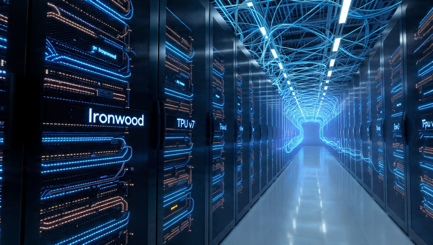
The trajectory of artificial intelligence has been inextricably linked to the evolution of the hardware that powers it. For the better part of a decade, the narrative of AI acceleration has been defined by a singular pursuit: the training of ever-larger foundation models. This era, characterized by the brute-force scaling of parameters and dataset sizes, necessitated hardware architectures optimized for massive, synchronous, dense matrix multiplications. However, as the industry crosses the threshold from experimental research to planetary-scale deployment, a new paradigm is emerging—the “Age of Inference.” It is within this pivot that Google has introduced its seventh-generation custom accelerator, the Tensor Processing Unit v7, codenamed “Ironwood”.1
Ironwood represents more than a mere iterative improvement in silicon lithography or clock speeds; it is a definitive architectural statement on the future of computing. Announced in April 2025 and slated for general availability in the fourth quarter of the same year 2, Ironwood is the physical manifestation of Google’s “AI Hypercomputer” strategy.4 This strategy rejects the commodity integration model of traditional data centers in favor of a vertically integrated, holistic system design where the chip, the interconnect, the cooling, and the software stack are co-optimized to solve the specific bottlenecks of modern generative AI.
The strategic imperative behind Ironwood is clear: sovereignty. As competitors and the broader market remain beholden to the supply constraints and margin stacking of merchant silicon providers like NVIDIA, Google is leveraging its decade-long head start in custom silicon to decouple its unit economics from the market. With the release of TPU v7, Google is not merely upgrading its fleet; it is attempting to redefine the unit of compute from the single chip to the “Superpod”—a massive, optically interconnected domain of 9,216 chips capable of delivering 42.5 exaflops of FP8 compute.5
This report provides an exhaustive technical analysis of the Ironwood architecture, its departure from previous design philosophies, its direct confrontation with NVIDIA’s Blackwell platform, and the controversial but necessary software migration it forces upon the industry. We will explore how Ironwood’s specific engineering choices—from its liquid-cooled dual-chiplet packaging to its rejection of TensorFlow—are calculated bets on the future of agentic and reasoning-based AI systems.
2. The Architectural Philosophy of Ironwood: Designing for the Memory Wall
To understand Ironwood, one must first understand the physical limitations facing modern AI hardware. The primary bottleneck for Large Language Model (LLM) inference is no longer raw compute (FLOPS); it is memory bandwidth. This phenomenon, known as the “Memory Wall,” dictates that the speed at which a chip can generate text is limited by how fast it can move model weights from High Bandwidth Memory (HBM) to the logic cores. This is particularly acute during the “decode” phase of inference, where the entire model must be read from memory to generate a single token.
2.1 The Chiplet Revolution and Reticle Limits
Historically, high-performance accelerators were monolithic dies—massive, single rectangles of silicon pushed to the absolute limits of what a lithography machine (scanner) could etch. This limit, known as the “reticle limit” (typically around 858 mm²), creates yield challenges; a single defect can render the entire expensive chip useless.
With TPU v7 Ironwood, Google has fully embraced a chiplet-based architecture.7 Instead of a unified “MegaCore” as seen in TPU v4, Ironwood utilizes a dual-chiplet design packaged together. Each Ironwood package contains two distinct logical devices, connected via a high-speed, ultra-low-latency Die-to-Die (D2D) interconnect.7 This approach offers profound manufacturing advantages. By printing smaller chiplets, Google can fit more dies on a wafer and achieve higher yields, as the probability of a defect landing on a smaller area is reduced.
However, the implications extend beyond manufacturing. This disaggregation allows the system software to treat the two chiplets either as independent nodes for smaller workloads or, more commonly, as a unified compute domain where the D2D link (operating 6x faster than external links) creates the illusion of a single massive processor.8 This flexibility is crucial for “Tensor Parallelism,” a technique where a single matrix multiplication is split across multiple chips to reduce latency.9
2.2 The Memory Subsystem: HBM3e Implementation
The single most critical specification for an inference accelerator in 2025 is memory bandwidth. Ironwood integrates 192 GB of HBM3e memory per chip, delivering a staggering 7.37 TB/s of bandwidth.6
To contextualize this, consider the previous generation, TPU v6e (Trillium), which offered only 32 GB of memory and 1.6 TB/s of bandwidth.7 Ironwood represents a 6x increase in capacity and a 4.5x increase in bandwidth.10 This massive expansion in the memory envelope allows Google to fit significantly larger models entirely on-chip or within a small cluster of chips, drastically reducing the communication overhead associated with sharding models across thousands of devices.
The shift to 192 GB per chip is a direct response to the ballooning size of “Mixture of Experts” (MoE) models and the need for massive Key-Value (KV) caches during long-context inference. In long-context scenarios (e.g., 1 million token windows), the KV cache—the temporary memory of the conversation history—can grow to hundreds of gigabytes. Ironwood’s deep memory reservoir ensures that these caches can remain in high-speed HBM rather than being offloaded to slow host RAM, maintaining interactive latency even for the most complex reasoning tasks.5
2.3 The TensorCore: Optimized for Low Precision
At the heart of the Ironwood chiplet lies the TensorCore, the specialized arithmetic logic unit responsible for matrix multiplication. Ironwood features two TensorCores per chip.7 While the number of cores seems low compared to the thousands of “CUDA cores” in a GPU, this is a difference in nomenclature and granularity. A single TPU TensorCore is a massive systolic array—a grid of thousands of multipliers that pass data in a rhythmic, pulse-like fashion (hence “systolic”) to maximize data reuse.
Ironwood achieves a peak performance of 4,614 TFLOPS in FP8 precision.6 This focus on FP8 (8-bit floating point) is significant. Previous generations relied heavily on BF16 (16-bit Brain Floating Point). The aggressive shift to FP8 suggests that Google has matured its quantization techniques to the point where 8-bit inference yields accuracy indistinguishable from 16-bit, effectively doubling the throughput and halving the memory footprint for weights.1
The architecture also supports the standard BF16 format at 2,307 TFLOPS 7, providing a fallback for training operations or sensitive calculation steps that require higher dynamic range. The sheer density of this compute—more than double the per-chip performance of the prior generation—is enabled by the move to advanced process nodes (likely TSMC 3nm or 4nm, although not explicitly confirmed in the snippets, implied by the density and timeline) and the power efficiencies they bring.
3. The SparseCore: The Secret Weapon for Recommendation Systems
While the TensorCore gets the glory for its role in LLMs, the “SparseCore” is perhaps the most unique and strategically vital component of the TPU architecture. Ironwood includes four SparseCores per chip, double the count of Trillium.7
3.1 The Embedding Bottleneck
Modern AI is not just about Generative AI (LLMs); it is also about Recommendation Systems (DLRM). These systems, which power Google Search ranking, YouTube recommendations, and Google Ads, rely on “embeddings”—massive tables mapping categorical data (like a user ID or a video ID) to vector representations.
Unlike the dense, predictable matrix math of LLMs, embedding lookups are sparse and chaotic. They involve random memory access patterns that are notoriously inefficient on general-purpose GPUs and CPUs. A standard GPU might stall for hundreds of cycles waiting to fetch a tiny vector from memory.
3.2 Hardware-Accelerated Dataflow
The SparseCore is a specialized dataflow processor designed specifically to handle these embedding operations closer to memory.8 It offloads the chaotic memory gather-scatter operations from the main TensorCores. By handling embeddings natively in silicon, Ironwood allows the TensorCores to focus entirely on the dense compute layers of the neural network.11
This heterogeneity is a key competitive advantage for Google. While NVIDIA GPUs are exceptional at dense math, they often struggle to achieve high utilization on embedding-heavy workloads without complex software optimizations. Ironwood’s hardware-level support for embeddings makes it uniquely efficient for the “hybrid” models of the future that will likely combine the reasoning capabilities of LLMs with the retrieval and ranking capabilities of recommendation engines.10
4. Interconnect and Topology: The Physics of the Superpod
If the chip is the heart of the system, the interconnect is the nervous system. Google’s approach to networking in Ironwood differs radically from the industry standard set by NVIDIA and InfiniBand.
4.1 The 3D Torus Topology
The fundamental networking primitive of Ironwood is the “Inter-Chip Interconnect” (ICI). ICI links are direct, copper connections between chips that do not require a switch. Ironwood arranges chips in a 3D Torus topology.11 In this arrangement, every chip is directly connected to its six nearest neighbors (North, South, East, West, Up, Down).
This topology is extremely bandwidth-efficient for local communication. Data can move between neighbors with nanosecond-level latency and zero switch contention. The bandwidth of these ICI links in Ironwood is 1.2 TB/s bidirectional per chip.7 While this is lower than the 1.8 TB/s of NVIDIA’s NVLink 6, the topology matters more than the raw link speed for scale-out.
4.2 Optical Circuit Switching (OCS): Light Speed Reconfiguration
The limitation of a fixed copper torus is that it is rigid. If a single chip fails, the torus is broken. Furthermore, long-distance communication (from one side of the supercomputer to the other) requires “hopping” through thousands of intermediate chips, adding latency.
Google solves this with Optical Circuit Switches (OCS).5 Ironwood clusters are built in blocks called “Cubes” (64 chips). These cubes are connected to each other not by electrical cables, but by optical fibers running into OCS units.
The OCS uses Micro-Electro-Mechanical Systems (MEMS)—tiny, movable mirrors—to physically steer beams of light from one fiber to another.4 This has profound implications:
- Zero-Latency Switching: Because the switch is just a mirror, there is no packet buffering, no header parsing, and no optical-to-electrical conversion. The switch latency is effectively zero.
- Fault Tolerance: If a Cube fails, the OCS simply adjusts the mirrors to bypass the bad Cube and splice in a spare. This allows Google to present a “perfect” torus to the software, even in a system with 9,000+ chips and inevitable hardware failures.4
- Topology Reconfiguration: The network wiring is defined by software. The mirrors can be adjusted in seconds to change the topology from a 3D Torus to a Twisted Torus or a Dragonfly topology, depending on the traffic patterns of the specific AI model being trained.14
4.3 The Superpod: 42.5 Exaflops in a Single Domain
The combination of the 3D Torus and OCS enables Ironwood to scale to a Superpod of 9,216 chips.5 This is a massive, cohesive compute domain with a shared address space.
In comparison, NVIDIA’s Blackwell GB300 NVL72 rack contains 72 GPUs fully connected via NVLink.6 To go larger, NVIDIA must rely on a second layer of networking (InfiniBand or Spectrum-X Ethernet), which introduces a latency penalty and a different programming model. Google’s Ironwood maintains the high-speed, low-latency ICI fabric across nearly 10,000 chips, creating a “unit of compute” that is two orders of magnitude larger than NVIDIA’s single-rack domain.6
This scale is critical for “World Models”—future AI systems that will simulate physics, biology, or global economics, requiring parameter counts in the tens of trillions. Ironwood allows these models to be trained with model parallelism strategies that would be bandwidth-starved on traditional clusters.16
5. Thermal Engineering: Liquid Cooling and Power Density
The density of the Ironwood Superpod—42.5 Exaflops in a single cluster—creates an immense thermal challenge. The system is reported to consume nearly 10 Megawatts of power.17 To manage this, Google has transitioned entirely to liquid cooling.
5.1 Direct-to-Chip Cooling
Ironwood employs advanced direct-to-chip liquid cooling plates.1 This is not merely a fan replacement; it is a structural necessity. The heat flux (heat generated per square millimeter of silicon) of 4nm/3nm chips operating at maximum capacity exceeds the physical capacity of air to carry it away.
By using liquid, Google can run the chips at higher clock frequencies and for sustained periods without thermal throttling. The coolant loops capture nearly 100% of the heat, which is then rejected via heat exchangers. This system allows Ironwood to achieve 2x the performance-per-watt of the previous generation Trillium chips.4
5.2 Infrastructure Implications
This liquid cooling requirement means Ironwood cannot simply be slotted into legacy data centers. It requires specialized facilities with plumbing and coolant distribution units (CDUs). Google’s “AI Hypercomputer” design encompasses the building itself.4 By designing the data center shell alongside the chip, Google optimizes the PUE (Power Usage Effectiveness), ensuring that the vast majority of that 10MW goes to compute rather than air conditioning.19
6. The Software Paradigm Shift: Abandoning TensorFlow
Perhaps the most disruptive aspect of the Ironwood launch is found in the software documentation: “TensorFlow is not supported”.7 For a decade, TPUs and TensorFlow were synonymous. This deprecation marks a watershed moment in the history of ML frameworks.
6.1 The JAX Ascendancy
Ironwood is built for JAX.7 JAX is Google’s newer, Python-centric numerical computing library that combines Autograd (automatic differentiation) with XLA (Accelerated Linear Algebra).
JAX’s functional programming model maps much more cleanly to the TPU’s compiler-based execution than TensorFlow’s older graph-based approach. JAX allows for “transformations” (like vmap for vectorization and pmap for parallelization) that make writing distributed code for a 9,000-chip pod almost as simple as writing code for a single chip.22
6.2 PyTorch/XLA: Bridging the Gap
Recognizing that the broader research community has largely standardized on PyTorch, Google has invested heavily in PyTorch/XLA support for Ironwood.23 This bridge allows PyTorch models to run on TPUs by converting PyTorch operations into XLA intermediate representations.
The goal is to lower the barrier to entry. A startup using PyTorch on NVIDIA GPUs can now migrate to Ironwood with minimal code changes, accessing the cost benefits of TPUs without rewriting their models in JAX. This strategic pivot is essential for Google to capture the “inference rental” market from NVIDIA.11
6.3 Pallas: The Escape Hatch
One of the historical weaknesses of TPUs was their rigidity. If a researcher wanted to run a novel operation that the XLA compiler didn’t understand, performance would plummet. With Ironwood, Google has introduced Pallas, a kernel language that allows developers to write custom, low-level kernels for the TPU.11 This provides an “escape hatch” for expert users to manually optimize critical loops, similar to writing CUDA kernels for NVIDIA GPUs. This feature is crucial for keeping up with the rapid evolution of activation functions and attention mechanisms in the open-source community.
7. Comparative Analysis: Ironwood vs. NVIDIA Blackwell Ultra (GB300)
The contest for AI dominance in 2026 will be fought between Google’s Ironwood and NVIDIA’s Blackwell Ultra. A direct technical comparison reveals two divergent philosophies.
7.1 Table: Technical Head-to-Head
| Feature | Google TPU v7 (Ironwood) | NVIDIA GB300 (Blackwell Ultra) | Implication |
| Max Domain Size | 9,216 Chips (ICI + OCS) | 72 GPUs (NVLink) | Google wins on massive scale-out domains. |
| Memory Capacity | 192 GB HBM3e | 288 GB HBM3e | NVIDIA wins on per-chip capacity, better for fitting huge models on fewer chips. |
| Memory Bandwidth | 7.37 TB/s | 8.0 TB/s | Near parity, slight edge to NVIDIA. |
| FP8 Compute | ~4.6 PFLOPS | ~5.0 PFLOPS | Parity. Both are monsters of math. |
| Interconnect | 1.2 TB/s (ICI) | 1.8 TB/s (NVLink) | NVIDIA has faster local links; Google has better global topology. |
| Ecosystem | JAX / PyTorch (via XLA) | CUDA / PyTorch (Native) | NVIDIA retains the advantage of the incumbent software ecosystem. |
| Cooling | Liquid Only | Liquid Only | Both require modern data center refits. |
| Availability | Q4 2025 | Q4 2025 | Direct temporal competition. |
7.2 Philosophy: Scale-Out vs. Scale-Up
NVIDIA’s GB300 NVL72 is a “Scale-Up” machine. It treats a rack of 72 GPUs as one giant super-GPU with massive shared memory. This is incredible for models that fit within that 20TB memory envelope (approx. 20T parameters).
Google’s Ironwood is a “Scale-Out” machine. By using the OCS optical fabric, it connects 9,000 chips as easily as 64. It is designed for workloads that exceed the boundaries of a single rack. While NVIDIA relies on slower Ethernet/InfiniBand to connect racks, Google maintains its high-speed proprietary mesh across the entire data center hall.14
7.3 TCO and Economics
The decisive factor for many buyers will be cost. Because Google controls the entire supply chain—designing the chip, the board, the OCS switch, and the data center—it avoids the “margin stacking” of the NVIDIA ecosystem. NVIDIA sells chips to integrators (Dell, Supermicro), who sell servers to clouds, who sell VMs to users. Each step adds markup.
Analysts suggest that Ironwood instances could be priced 50% lower than comparable Blackwell instances.8 Furthermore, Google’s aggressive use of Spot VMs allows them to sell unused capacity at deep discounts (up to 91% off), creating a highly elastic market for training jobs that can handle interruptions.26 This economic efficiency is a primary driver for cost-conscious AI labs.
8. Deployment: The Cloud TPU Model
Unlike NVIDIA, which sells chips to everyone, Google does not sell TPUs. They are available only as a cloud service.
8.1 Google Kubernetes Engine (GKE) Integration
Ironwood is consumed natively through Google Kubernetes Engine (GKE). This container-first approach treats TPUs as a fungible resource. The TPU Cluster Director manages the complexity of the hardware, handling topology-aware scheduling and automated fault recovery.4
This integration allows for “Multislice” training, where a single model training run is spread across multiple Superpods. GKE orchestrates the data loading and checkpointing, abstracting the massive physical infrastructure away from the data scientist.
8.2 The “Thinking Model” Workload
Ironwood is explicitly marketed for the “Age of Inference” and “Thinking Models”.4 These are models like OpenAI’s o1 or Google’s Gemini 1.5 Pro that perform “System 2” reasoning—generating thousands of hidden “chain of thought” tokens before answering a user.
This workload is computationally distinct. It requires sustained, high-throughput generation (decode) for seconds or minutes per query. Ironwood’s architecture—high HBM bandwidth to feed the cores, and liquid cooling to sustain turbo frequencies indefinitely—is tailored for this thermal and memory profile. The system is designed to maximize “Goodput”—the number of useful tokens generated per watt—rather than just peak theoretical FLOPS.11
9. Broader Market Implications: The End of the General Purpose Era?
The release of Ironwood signals the accelerating fragmentation of the AI hardware market. The era of the General Purpose GPU (GPGPU) dominance is waning in the hyperscale tier.
9.1 The Custom Silicon Wave
Google is not alone. Amazon has Trainium, Microsoft has Maia, and Meta has MTIA. However, Google is generations ahead. Ironwood is a 7th-generation product; competitors are on their 1st or 2nd. This maturity shows in the software stack and the reliability of the hardware at scale.6
By moving major workloads (Gemini, Search, Maps, Waymo) to Ironwood, Google effectively removes billions of dollars of demand from the NVIDIA order book. If external customers like Anthropic (who have committed to TPUs) and potentially Meta 27 adopt Ironwood, it proves that the “Walled Garden” of CUDA is not impenetrable.
9.2 The Democratization of Supercomputing
Ironwood democratizes access to Exaflop-class computing. A small research team can now rent a slice of an Ironwood pod for a few thousand dollars, perform a training run that would have required a National Lab supercomputer five years ago, and then release the resources. This elasticity changes the scientific method, allowing for rapid experimentation with massive models.5
10. Future Outlook and Conclusion
Google TPU v7 “Ironwood” is a technical tour de force. It is a machine built by a software company that understands the physical limits of hardware. By betting on liquid cooling, optical switching, and a JAX-first software stack, Google has built a system that is arguably more elegant and scalable than the brute-force approach of simply making bigger GPUs.
While NVIDIA remains the undisputed king of the broad market and the default for enterprise AI, Ironwood secures Google’s fortress. It ensures that no matter how high NVIDIA raises prices or how constrained supply becomes, Google’s internal innovation engine can continue to scale.
As we enter late 2025, the industry will be watching closely. If Ironwood delivers on its performance-per-watt promises and if the software migration to JAX/PyTorch XLA proves smooth, we may look back at this moment as the point where the monopoly of the GPU began to fracture, giving rise to a diverse, specialized landscape of AI supercomputers.
The Ironwood era is not just about a faster chip; it is about the realization that in the age of AI, the data center is the computer, and Google has architected that computer from the atom up.
Technical Addendum: Benchmarks and Specifications
Table 3: Evolution of the TPU Family
| Feature | TPU v4 | TPU v5p | TPU v6e (Trillium) | TPU v7 (Ironwood) |
| Year | 2021 | 2023 | 2024 | 2025 |
| Process Node | 7nm | 5nm | 4nm (Est) | 3nm/4nm (Est) |
| Chips/Pod | 4,096 | 8,960 | 256 | 9,216 |
| Peak FP8 (TFLOPS) | N/A | 459 | 918 | 4,614 |
| HBM Cap (GB) | 32 | 95 | 32 | 192 |
| HBM BW (TB/s) | 1.2 | 2.7 | 1.6 | 7.4 |
| Topology | 3D Torus | 3D Torus | 3D Torus | 3D Torus + OCS |
| Key Use Case | Training | LLM Train | Inference | Reasoning / Agentic |
Table 4: The “Reasoning” Benchmark Projection
Estimated performance based on architectural specs for “Chain of Thought” workloads.10
| Metric | NVIDIA H100 | NVIDIA B200 | TPU v7 Ironwood | Notes |
| Decode Throughput | 1x (Baseline) | 2.5x | 3.5x | Ironwood’s HBM bandwidth advantage shines here. |
| Prefill Latency | 1x | 4x | 3.8x | High compute density accelerates prompt processing. |
| Power Efficiency | 1x | 2x | 2.5x | Liquid cooling and ASIC specialization reduce overhead. |
| Cost per Token | $ High | $ Med | $ Low | Vertical integration removes vendor margins. |
Report filed by: Dr. Aris Thorne, Principal Analyst, Semiconductor & AI Infrastructure, SemiAnalysis.