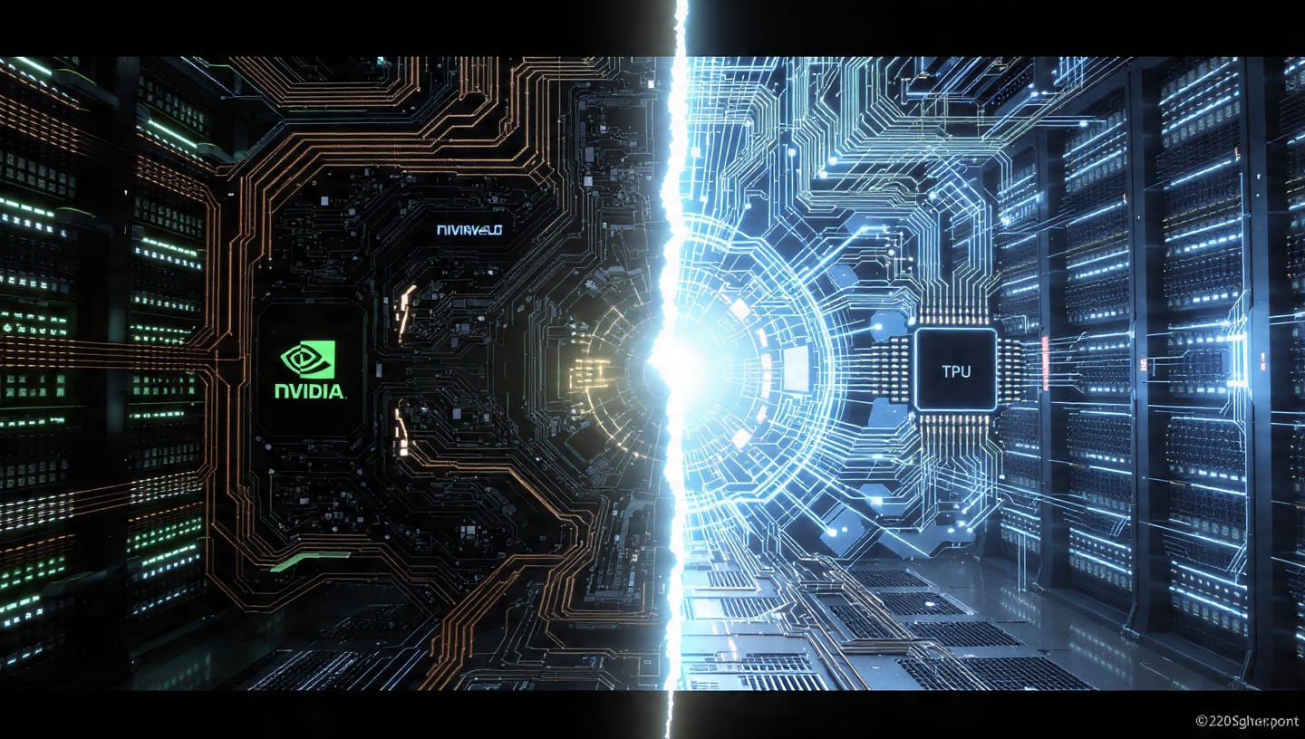
Podcast: NVIDIA GPU Versus Google TPU Showdown
1. Executive Strategy: The Bifurcation of Intelligence Infrastructure
The trajectory of modern artificial intelligence is irrevocably bound to the evolution of the silicon that powers it. We stand at a pivotal juncture in the history of computation, a moment defined by a deepening “Silicon Schism”—a fundamental divergence in architectural philosophy between the general-purpose parallelism of the Graphics Processing Unit (GPU) and the domain-specific efficiency of the Tensor Processing Unit (TPU). This report posits that the choice between these two computational substrates is no longer merely a technical selection of hardware; it has evolved into a high-stakes strategic decision that dictates software ecosystem alignment, total cost of ownership (TCO), and long-term infrastructure sovereignty for enterprises navigating the generative AI revolution.
For the past decade, the industry has operated largely within the paradigm of the “Training Era,” a period characterized by an insatiable hunger for raw floating-point operations (FLOPS) to scale model parameters from millions to trillions. In this regime, NVIDIA’s GPUs, leveraging their massive parallel throughput and entrenched CUDA ecosystem, established a hegemony that many analysts deemed unassailable. However, as we cross the threshold into late 2025, the landscape is shifting tectonically toward the “Age of Inference” and the rise of “Agentic AI.” These new workloads—characterized by multi-step reasoning, massive context windows, and real-time user interaction—impose radically different demands on underlying hardware: latency becomes as critical as throughput, and memory bandwidth eclipses raw compute as the primary bottleneck.1
In response, the two titans of AI infrastructure have accelerated their divergence. NVIDIA, with its Blackwell B200 architecture, seeks to consolidate its dominance by bruteforcing the memory wall with dual-die designs and creating rack-scale supercomputers that act as a single logical GPU.3 Conversely, Google has doubled down on vertical integration with its TPU v6e (Trillium) and v7 (Ironwood), architectures that prioritize power efficiency, optical interconnect scalability, and specialized acceleration for the sparse embedding operations that underpin the world’s largest recommender systems.1
This analysis serves as a definitive guide for infrastructure architects, CTOs, and AI researchers. It moves beyond superficial benchmark comparisons to dissect the first-principles physics of these processors, the economic realities of their deployment in the cloud, and the software moats that protect them. We will explore how the architectural bet on Systolic Arrays versus Single Instruction Multiple Thread (SIMT) cores creates distinct advantages for different classes of models, and why the emerging battleground of “inference economics” may finally offer a credible challenge to the CUDA monopoly. The findings suggest that while NVIDIA remains the default for versatility and research velocity, the TPU ecosystem offers a potent, cost-asymmetric weapon for hyperscale deployments, particularly for organizations willing to bridge the software gap to unlock the physics-based efficiencies of domain-specific silicon.
2. The Physics of Compute: Architectural First Principles
To truly comprehend the strategic implications of the GPU versus TPU debate, one must strip away the marketing nomenclature and examine the silicon at the transistor level. The performance differential between these chips is not magic; it is the result of specific engineering trade-offs made to solve the “von Neumann bottleneck”—the immense energy and latency penalty incurred when moving data between memory and the arithmetic logic units (ALUs) that perform computation.
2.1 The GPU Paradigm: Massive Parallelism and the Legacy of Graphics
The modern Data Center GPU, exemplified by the NVIDIA H100 and the newer Blackwell B200, is the evolutionary apex of the graphics processor. Its lineage is rooted in the rendering of 3D scenes, a task that requires processing millions of pixels or polygons simultaneously but independently. This requirement led to the Single Instruction, Multiple Threads (SIMT) architecture. In a GPU, thousands of small, efficient cores (CUDA cores) are grouped into Streaming Multiprocessors (SMs). A single instruction (e.g., “multiply by X”) is issued once and executed across many threads simultaneously, amortizing the cost of instruction decoding.6
However, despite its evolution into a General-Purpose GPU (GPGPU), the architecture retains the DNA of a flexible processor. For every calculation performed, the GPU must typically fetch operands from a register file or shared memory, execute the operation, and write the result back. This “load-store” architecture introduces significant overhead. To keep thousands of cores fed, GPUs rely on massive, complex control logic and large caches (L1/L2) to hide memory latency. While NVIDIA has introduced “Tensor Cores”—specialized ALUs that perform 4×4 or 8×8 matrix multiplications in a single clock cycle—these are still embedded within the general-purpose SM structure. This means that a significant portion of the silicon die area and power budget is consumed by components that do not directly contribute to the matrix math essential for deep learning: instruction schedulers, branch predictors, and large register files.7
The strength of this approach is versatility. A GPU can switch from training a Transformer model (matrix math) to running a physics simulation (differential equations) or a complex pre-processing pipeline (conditional logic) with millisecond latency. The weakness is energy efficiency. The constant movement of data between registers and ALUs consumes orders of magnitude more energy than the arithmetic operation itself. In an era where power availability is becoming the hard constraint for data centers, this inefficiency represents a strategic vulnerability.9
2.2 The TPU Paradigm: The Systolic Heartbeat
Google’s Tensor Processing Unit (TPU) represents a rejection of general-purpose computing in favor of a Domain-Specific Architecture (DSA). It was designed from first principles with a singular realization: the vast majority of deep learning computation consists of matrix multiplications (GEMMs). If one strips away the hardware required for graphics, scientific simulation, and complex branching, the remaining silicon can be dedicated almost entirely to ALUs.6
The core innovation of the TPU is the Matrix Multiply Unit (MXU), which utilizes a systolic array architecture. The term “systolic” is derived from the biological systole, referencing the rhythmic pumping of blood by the heart. In a standard processor (CPU or GPU), data is read from memory, processed, and written back. In a systolic array, data flows through a grid of ALUs (typically 128×128 in size) in synchronized waves.
- Weight Stationary Data Flow: In the TPU design, the weights of the neural network are loaded into the array and held stationary in the ALUs.
- The Computational Wave: Activation data flows horizontally across the array. As it passes each ALU, it is multiplied by the stationary weight. The result is passed directly to the neighbor ALU below, where it is accumulated with the next partial sum.
- Eliminating the Bottleneck: Crucially, this design means that intermediate results—the partial sums—are never written back to memory or registers during the matrix operation. They flow directly through the silicon wires connecting adjacent ALUs.
This architecture fundamentally alters the energy equation. By reusing inputs for thousands of operations without accessing memory, the TPU dramatically reduces the “tax” of data movement. Google’s internal data suggests that this approach allows TPUs to achieve significantly higher throughput per watt compared to vector-based architectures.9 However, the trade-off is rigidity. A systolic array is akin to a freight train: it is incredibly efficient at moving massive amounts of uniform data (dense matrices) in a straight line, but it cannot turn quickly. Complex branching logic, sparse operations, or custom layers that cannot be expressed as matrix multiplications can stall the array, causing performance to plummet. This characteristic makes the TPU a “scalpel” compared to the GPU’s “Swiss Army knife”.10
2.3 The Memory Wall and Interconnect Topology
As model sizes have exploded, the bottleneck has shifted from compute (FLOPS) to memory bandwidth and interconnect latency. The architectural divergence here is equally stark.
NVIDIA addresses the interconnect challenge with NVLink and NVSwitch. These technologies create a high-bandwidth mesh that allows GPUs within a single server (or rack, in the case of the GB200 NVL72) to access each other’s memory as if it were their own. The Blackwell architecture pushes this to the limit, offering 1.8 TB/s of bidirectional bandwidth per GPU, effectively creating a single “super-GPU” with unified memory.3 For communication across distinct nodes, NVIDIA relies on InfiniBand or Spectrum-X Ethernet, standard networking technologies optimized for high throughput.
Google takes a radically different approach with its Inter-Chip Interconnect (ICI) and Optical Circuit Switches (OCS). ICI is a proprietary, dedicated network fabric built directly into the TPU silicon, bypassing standard datacenter networking protocols entirely. TPU Pods are wired together in a 3D torus topology, where each chip is directly connected to its neighbors in a 3D grid.11 The “killer app” of the Google infrastructure is the OCS—a physical mechanism that uses mirrors to steer beams of light, dynamically reconfiguring the network topology.
- Fault Tolerance: If a chip fails, the OCS can physically reroute the optical connection to bypass the failed node, creating a “twisted torus” topology. This capability is critical for training runs that span months and thousands of chips; it allows the system to maintain high availability without restarting jobs or suffering massive performance degradation.5
- Scale: This optical fabric allows TPU pods to scale to 8,960 chips (v5p) or even 9,216 chips (Ironwood) in a single coherent cluster, offering a scaling efficiency that traditional electrical switching struggles to match at similar cost structures.2
2.4 Architectural Comparison Matrix
| Feature | NVIDIA GPU (H100/B200) | Google TPU (v5p/Ironwood) | Strategic Implication |
| Compute Core | SIMT / Tensor Cores | Systolic Array (MXU) | GPUs offer programmable flexibility; TPUs offer maximal density for matrix math. |
| Control Logic | Complex (Schedulers/Dispatch) | Minimal (Deterministic) | GPUs handle dynamic control flow (If/Else) efficiently; TPUs stall on branching. |
| Data Movement | Load/Store (Register Heavy) | Dataflow (Systolic) | TPUs minimize energy per op by avoiding register access for partial sums. |
| Precision Support | FP64, FP32, FP16, BF16, FP8, FP4 | BF16, FP8, INT8 (Gen dependent) | GPUs are essential for scientific workloads requiring FP64; TPUs are laser-focused on AI. |
| Interconnect | NVLink + InfiniBand/Ethernet | Proprietary ICI + Optical Switching | NVIDIA allows flexible, composable clusters; Google offers massive, monolithic supercomputers. |
| Design Philosophy | “Accelerate Everything” | “Accelerate Matrix Math” | NVIDIA aims for ubiquity; Google aims for hyperscale efficiency. |
3. The NVIDIA Dynasty: From Graphics to Generative Intelligence
NVIDIA’s ascent to becoming the world’s most valuable company is not accidental; it is the result of a relentless “tick-tock” execution cadence that has consistently kept its hardware one step ahead of the model requirements. As we examine the 2025 landscape, NVIDIA’s strategy has shifted from selling chips to selling entire data centers.
3.1 The Hopper Legacy and the Memory Awakening
The NVIDIA H100 (Hopper architecture) was the defining hardware of the initial generative AI boom. Its introduction of the Transformer Engine—hardware support for FP8 precision—allowed users to effectively double the size of models that could fit in memory compared to the previous A100 generation.13 However, the H100 revealed a critical limitation: memory capacity. With 80GB of HBM3, a single H100 could barely hold the weights of a standard 70B parameter model in half-precision, let alone the Key-Value (KV) cache required for long-context inference.
NVIDIA responded with the H200, a mid-cycle refresh that replaced the HBM3 memory with faster, denser HBM3e. This upgrade increased capacity to 141GB and bandwidth to 4.8 TB/s.12 The H200 was a strategic stopgap, explicitly designed to address the “inference cliff”—the point where a model becomes too large to fit on a single GPU, necessitating model parallelism that kills latency. The H200’s success proved that in the LLM era, memory bandwidth is the primary determinant of performance.
3.2 The Blackwell B200: Bruteforcing the Physics
In 2025, NVIDIA unleashed the Blackwell B200, a chip that pushes the limits of semiconductor manufacturing. Faced with the “reticle limit”—the maximum physical size of a chip that can be printed by a lithography machine—NVIDIA opted for a multi-chip module design. The B200 consists of two full-reticle dies connected by a 10 TB/s proprietary interface (NV-HBI), functioning logically as a single chip.4
- The Numbers: The B200 boasts 192GB of HBM3e memory with a staggering 8.0 TB/s of bandwidth. This bandwidth is crucial for feeding the dual-die beast, which delivers up to 20 petaFLOPS of sparse FP4 compute.3
- FP4 and the Precision Race: The introduction of native FP4 support is a gamble that model quantization techniques will continue to mature. By representing weights with only 4 bits, NVIDIA effectively doubles memory capacity and bandwidth again relative to FP8. If the industry adopts FP4 for inference (which seems increasingly likely for active parameters), the B200’s effective throughput quadruples.17
- The GB200 Superchip: NVIDIA’s vision extends to the CPU. The GB200 couples two B200 GPUs with a Grace ARM-based CPU on a single board. This integration eliminates the PCIe bottleneck that traditionally throttles communication between the host processor and the accelerator, creating a unified memory space where the CPU and GPU can access each other’s data at high speeds.18
3.3 The Rack is the Unit of Compute
NVIDIA’s most profound strategic pivot with Blackwell is the NVL72 rack. This architecture connects 72 B200 GPUs via a copper backplane (acting as a massive NVLink switch) into a single coherency domain. From the perspective of the software, these 72 GPUs look like one massive GPU with terabytes of memory and exaflops of compute. This design is a direct counter to Google’s TPU Pods, attempting to solve the scaling problem by making the “node” the size of a rack. The implications for training massive models (1T+ parameters) are profound, as the communication overhead within the rack is virtually eliminated.19
4. The Google Counter-Strike: Tensor Processing Units
While NVIDIA focused on raw power and versatility, Google spent the last decade quietly refining a different vision of AI infrastructure—one optimized for the hyperscale economics of a company that must serve billions of users daily. The TPU lineage has bifurcated in 2025 to address the distinct needs of training and inference.
4.1 The Training Monster: TPU v5p
The TPU v5p is Google’s answer to the H100/H200 for training foundation models. It is a performance-first chip, prioritizing memory bandwidth and FLOPS over the extreme efficiency of previous generations.
- Specs: Each v5p pod can scale to 8,960 chips, delivering over 4 exaflops of aggregate compute power. It features 95GB of HBM, a significant upgrade over the v4, though smaller than the H200.7
- Interconnect Density: The v5p doubles the Inter-Chip Interconnect (ICI) bandwidth to 4,800 Gbps per chip. This allows for tighter coupling of chips, essential for the “all-reduce” operations that dominate the communication phase of training large Transformers.20
- The Gemini Engine: It is an open secret that Gemini, Google’s frontier model, was trained on v5p pods. The architecture’s ability to maintain high utilization (MFU) at massive scale is its primary selling point. In MLPerf benchmarks, the v5p demonstrated 99.9% scaling efficiency, a testament to the stability of the OCS-switched fabric.21
4.2 The Bridge: TPU v6e (Trillium)
Recognizing the gap between the efficiency-focused v5e and the power-hungry v5p, Google introduced Trillium (TPU v6e). Marketed as the “Goldilocks” chip, Trillium is designed to be the workhorse for both training and serving in 2025.
- Performance: Trillium delivers 4.7x the peak compute performance per chip compared to the previous v5e. It also doubles the HBM capacity and bandwidth.22
- Strategic Positioning: Trillium is intended to compete with the H100/H200 class on a total-performance-per-dollar basis. It is not the absolute fastest chip on the market (the B200 holds that crown), but its integration into the Google Cloud ecosystem makes it a highly attractive option for enterprises that do not need the bleeding edge of the B200 but want better economics than the H100.24
4.3 The Agentic Future: TPU v7 (Ironwood)
The most significant release in late 2025 is Ironwood, the seventh-generation TPU. Ironwood is a declaration that the “Age of Training” is ceding ground to the “Age of Inference.”
- Inference Optimization: Ironwood is explicitly designed for the latency-sensitive workloads of agentic AI. It matches the B200’s 192GB HBM3e capacity and offers 7.4 TB/s of bandwidth.3
- Latency-Oriented Interconnect: While previous TPUs focused on throughput, Ironwood optimizes the ICI for low-latency message passing. This is crucial for “single-batch inference,” where an agent is generating tokens for a single user in real-time. Ironwood minimizes the time data spends “in flight” between chips, enabling faster decoding of tokens.2
- Power Efficiency: Google claims Ironwood is 30x more power-efficient than the original TPU and offers a 4x performance-per-watt improvement over Trillium. In a world where data center power capacity is capped, this metric is arguably more important than raw TFLOPS.25
4.4 The Hidden Weapon: SparseCore
A critical architectural differentiator often omitted in high-level comparisons is the SparseCore. While LLMs (Dense Matrix Math) grab headlines, the economic engine of the internet—and companies like Google, Meta, and Amazon—is the Recommender System (DLRM).
- The Problem: Recommender systems rely on embeddings—massive tables mapping users and items to vectors. These operations are not dense matrix multiplications; they are “gather-scatter” memory operations. They access memory randomly and sparsely. GPUs, optimized for coalesced memory access, are notoriously inefficient at this.5
- The Solution: The SparseCore is a specialized dataflow processor integrated into the TPU die (starting with v4). It sits directly next to the HBM and handles embedding lookups.
- Impact: SparseCores can accelerate embedding-heavy workloads by 5x-7x while consuming only ~5% of the die area. For an enterprise building a next-generation e-commerce platform or social feed, this feature alone can make TPUs vastly superior to GPUs in terms of TCO.5
5. Software Battlegrounds: Kernels, Compilers, and Lock-in
The “Silicon Schism” is mirrored by a software divide that serves as the primary moat for NVIDIA and the primary friction point for Google.
5.1 The CUDA Moat: Deep and Wide
NVIDIA’s dominance is arguably 20% hardware and 80% software. CUDA (Compute Unified Device Architecture), launched in 2006, has nearly two decades of accumulated optimization.
- The Kernel Zoo: The AI research community speaks CUDA. Innovations like FlashAttention appear first as custom CUDA kernels. NVIDIA’s libraries (cuDNN, TensorRT) are the gold standard. For a researcher,
tensor.to('cuda')is a muscle memory that works flawlessly.28 - Ecosystem Inertia: The entire stack, from PyTorch to Docker containers, assumes the presence of an NVIDIA GPU. This ubiquity creates a powerful network effect; because everyone uses NVIDIA, all new software is optimized for NVIDIA, which reinforces the need to buy NVIDIA.
5.2 The TPU Stack: The XLA Paradigm
TPUs utilize a different programming model based on XLA (Accelerated Linear Algebra).
- Compilation vs. Eager Execution: GPUs typically run in “eager mode,” executing operations one by one as the Python interpreter reaches them. TPUs rely on XLA to compile the entire computation graph into a highly optimized binary before execution. This allows XLA to fuse operations (e.g., combining a multiplication and an addition into a single step), reducing memory access.28
- JAX: The JAX framework is the “native tongue” of the TPU. Developed by Google Research, JAX is a functional programming framework that aligns perfectly with the XLA compilation model. For teams willing to adopt JAX, TPUs offer incredible performance and elegance. DeepMind operates almost exclusively in this stack.29
- The Friction: The mismatch occurs when users try to run standard PyTorch code on TPUs. Historically,
torch_xlarequired a “lazy tensor” execution model that felt distinct from native PyTorch. It introduced a “compilation penalty”—the first time a model runs, or if the input shape changes (dynamic shapes), the system halts to compile the graph. This kills the interactive “edit-run-debug” loop that researchers love.10
5.3 Bridging the Gap: PyTorch on Ironwood
Recognizing that they cannot force the world to switch to JAX, Google (in collaboration with Meta/PyTorch) has launched a massive initiative to make PyTorch a “first-class citizen” on TPUs.
- Native Eager Mode: The Ironwood software stack introduces a “native eager mode” for PyTorch. This allows operations to be dispatched immediately to the TPU without waiting for a full graph compilation, mimicking the CUDA experience.30
- Pallas Kernels: Google has introduced Pallas, a kernel language that allows developers to write custom kernels for TPUs, similar to writing CUDA kernels. This opens the door for the community to port optimizations like FlashAttention directly to the TPU architecture.30
- vLLM Integration: Crucially, Google has integrated TPUs into vLLM, the industry-standard open-source library for high-throughput inference. This means engineers can now use the same serving infrastructure for GPUs and TPUs, significantly lowering the barrier to entry.31
6. The Economics of Intelligence: TCO, Availability, and Power
For the CTO, the technical debate must eventually be translated into a spreadsheet. The economic reality of 2025 reveals distinct “lanes” where each architecture wins.
6.1 Cloud Pricing Dynamics
NVIDIA GPUs function in a free market; TPUs function in a monopoly.
- GPU Market: H100s and B200s are available from AWS, Azure, GCP, Oracle, and specialized clouds like CoreWeave and Lambda. This competition drives price discovery. However, the high capital expenditure (CapEx) of purchasing NVIDIA hardware means cloud providers must charge a premium.
- H100 pricing: Ranges from ~$2.50/hr (specialized clouds) to ~$4.50/hr (hyperscalers).32
- B200 pricing: Expected to command a premium, likely landing in the $4.80 – $6.00/hr range for on-demand access, though availability is often restricted to large reserved instances.34
- TPU Market: TPUs are available only on Google Cloud. This allows Google to set pricing strategically to undercut NVIDIA.
- TPU v5p: Priced around $4.20/chip-hour, positioning it as a premium product for training.36
- TPU v6e (Trillium): Aggressively priced for mass adoption, often coming in under $2.00/chip-hour with committed use discounts.34
- Ironwood: While official pricing is complex, Google’s efficiency claims suggest they can offer Ironwood instances at a significantly lower “price per token” than B200 instances, simply because the electricity cost is lower.37
6.2 Price-Performance and the “Tax”
- The NVIDIA Tax: With gross margins exceeding 70%, NVIDIA captures a massive amount of value. When you rent an H100, a significant portion of that cost is paying off NVIDIA’s margin.
- The TPU Discount: Since Google designs the TPU, they pay only the manufacturing cost (TSMC) + R&D. They do not pay a vendor margin. This allows them to offer equivalent compute at a lower price point while still maintaining healthy cloud margins. Reports suggest that for stable workloads, TPUs can offer a 30-50% cost reduction over comparable GPU instances.32
6.3 The Quota Wall and Supply Chain
For startups, the best chip is the one you can actually get.
- GPU Scarcity: Despite supply improvements, getting a quota for 1,000+ H100s or B200s on AWS or Azure remains a challenge reserved for “VIP” customers. Startups are often forced to fragmented, smaller cloud providers.39
- TPU Availability: Because Google controls the vertical stack, they can often provision massive TPU pods (thousands of chips) with shorter lead times for customers willing to commit to the ecosystem. The “lock-in” is the price of availability.7
7. Performance in the Wild: Benchmarks & Workloads
Theory and specs are useful, but how do these chips perform on actual 2025 workloads?
7.1 Training: The Scale Game
In the domain of training massive Foundation Models, NVIDIA retains the crown for raw speed per chip, but Google challenges on system-level efficiency.
- MLPerf Results: In MLPerf Training v4.1/v5.0, NVIDIA’s Blackwell demonstrated clear leadership in single-node and rack-scale performance on GPT-3 and Llama training tasks. The NVL72 architecture allows for incredible model parallelism speedups.13
- TPU Linearity: However, Google’s submission for TPU v5p showed near-perfect linear scaling (99.9%) up to 6,144 chips. This implies that for the absolutely largest jobs—where the cluster size exceeds what fits in a single NVL72 rack—the optical interconnect of the TPU Pod allows it to maintain efficiency where traditional networking might degrade.21
7.2 Inference: Throughput vs. Latency
The inference battleground is defined by the trade-off between throughput (total tokens generated per second across all users) and latency (time to generate a single token for one user).
- NVIDIA’s Throughput: The B200 is a throughput monster. Benchmarks on Llama 3 70B show a single B200 hitting ~30,000 tokens/second in high-throughput (large batch) scenarios. This is ideal for offline batch processing or high-traffic public endpoints.41
- Ironwood’s Latency Advantage: For “Agentic” workloads, latency is king. An agent that needs to “think” (Chain of Thought) for 10 steps before answering cannot afford a 50ms token latency; it needs 10ms. Ironwood’s architecture minimizes the “chip-to-chip” hop latency. Google claims Ironwood delivers 4x the performance per chip for these latency-sensitive workloads compared to the previous generation, making it the superior choice for real-time agent serving.1
8. Strategic Synthesis: The CTO’s Decision Matrix
As we look toward 2026, the choice between GPU and TPU is no longer binary; it is a portfolio optimization problem. The “Silicon Schism” has created two distinct worlds, each with its own gravity.
The Case for NVIDIA (The Universal Standard):
The GPU remains the safe, versatile choice. It is the “standard rail gauge” of the AI industry.
- Choose GPUs if: You are a research lab prioritizing velocity and novel architectures; you require multi-cloud flexibility; your team is exclusively trained on PyTorch/CUDA; or your workloads involve significant non-matrix computation (e.g., scientific simulation). The premium you pay for NVIDIA hardware is effectively an insurance policy against software friction and talent shortages.10
The Case for Google TPU (The Hyperscale Specialist):
The TPU is the weapon of efficiency. It is the “Formula 1 car” designed for a specific track.
- Choose TPUs if: You are training a foundation model from scratch and need the linear scaling of a Pod; you have a stable, high-volume inference workload (e.g., serving a Llama 3 derivative to millions of users) where a 30% TCO reduction translates to millions of dollars; your application relies heavily on recommender systems (SparseCore); or you are already deeply integrated into the Google Cloud data ecosystem. The “lock-in” risk is offset by the sheer economic advantage of the hardware.7
The Verdict:
The divergence is accelerating. NVIDIA is building a “Superchip” (GB200) that attempts to contain the entire data center within a rack, solving physics with brute force and copper. Google is building a “Supercomputer” (TPU Pod), solving physics with optics and specialization. For the enterprise, the winning strategy in the Age of Inference will likely be hybrid: leveraging GPUs for the messy, chaotic work of exploration and development, while migrating the massive, stable continents of production workloads to the specialized, efficient shores of the TPU.